OSE PHD Students Yasser Silani and Forrest Hubert Craft High Tech Microscope from Scratch
Departmental News
Posted: August 26, 2019
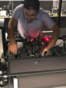
It took two years and a lot of trial and error but two researchers at The University of New Mexico Center for High Tech Materials (CHTM) have built "from scratch" a Stimulated Emission Depletion (STED) microscope, capable of imaging objects less than 100 nanometers in size.
Among the microscope’s applications is the ability to record high-resolution images of nano-sized biological specimens such as flu or HIV viruses, which a conventional optical microscope can’t do.
“Nano” is a unit prefix meaning one-billionth. To put that size in perspective, a strand of hair is about 80,000 to 100,000 nanometers wide, and a sheet of paper is approximately 100,000 nanometers thick.
The microscope was built by Yaser Silani and his colleague, Forrest Hubert, in the Quantum Nanophotonics & Biosensing Lab at the CHTM. Both are pursuing doctorates in Optical Science and Engineering.
Basically, the STED microscope allows researchers to see infinitesimally small objects better than other technology.
“Most dangerous and infectious viruses like flu and HIV, which are about 120 nanometers in size, cannot be identified under regular microscopes, but our STED microscope’s resolution is high enough to allow us to observe them,” Silani explained.
STED microscopy is a well-known technique to increase the resolution in optical microscopes. Like all other super-resolution imaging techniques, in STED microscopy samples, such as cells, must be first labeled or tagged with nano-size fluorescent molecules (usually less than 20 nanometers) acting as contrast agents which can shine lights upon being exposed to a laser. Simultaneously and at the same location that the first laser is applied to turn on those molecules, another one with a larger wavelength and a doughnut-shape profile (called STED beam) is applied.
This second laser can extinguish or inhibit the lights of those molecules everywhere except at the center of the doughnut where the laser intensity is zero. In other words, the fluorescent spot size of each label/tag is narrowed down to dimensions much smaller than the diffraction limit, typically 200 nanometers, and therefore, the resolution is improved. Then, by collecting the lights coming from those fluorescent molecules attached to a sample, a high-resolution 3D image of it is built up in STED microscopy, he explained.
However, the high power of the STED beam needed to shrink down the fluorescent spot of each label and reach the desired high resolution can be detrimental to the biological samples, as well as having other disadvantages. Silani and Hubert found that using silicon impurities in diamond crystals as labels in STED microscopy allows high resolutions to be achieved using lower power laser light.
It’s possible to just buy a STED microscope but it’s expensive – upwards of $1 million. Making their own was less expensive and allowed the researchers to get a better insight into the fundamental physics behind the technology and made it more convenient for them to modify the apparatus to their specific needs and reduce maintenance and repair costs, Silani said.
The most expensive part was a laser source, with a price tag of about $60,000. All the other parts were purchased from various vendors for under $15,000.
“The ability to build this microscope domestically can reduce its costs and consequently make it more affordable for places where this kind of microscope is highly needed, like research and development sections in clinics and hospitals,” Silani added.
“Because this was our first experience in the field of optical microscopy, we had many ups and downs not only in building the set-up but also in interpreting the data we took. Some of our challenges were preparing diamond samples with criteria necessary for our experiment, modifying and re-aligning the optical setup many times, and reproducing and analyzing the data. Our advisor, Professor Victor Acosta, helped us a lot from the first to the last step of this research. He is very knowledgeable in the area and we always use his advice to move our researches forward,” Silani said.
Having such a useful high-resolution microscope at CHTM puts UNM among the top universities that have this resource in their research tool bag and opens exciting and lucrative future opportunities, Silani said.
"We have already started to collaborate with researchers at the Center for Integrated Nanotechnologies and Sandia National Lab to use our microscope to image nanoscale arrays of SiV centers for applications in quantum information science," he noted.
