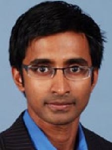
OSE Seminar by Dr. Ganesh Balakrishnan on Studying Dislocation Networks Using Transmission Electron Microscopy for Novel Optoelectronic Devices
Departmental News

Posted: April 28, 2021
Date: Thursday, April 29, 2021
Time: 11:00 AM to Noon
Location: via Zoom
Abstract:
The growth of GaSb on GaAs and silicon is of interest for a variety of scientific and technological applications including lasers, detectors, and solar cells. In the case of GaSb grown on GaAs, some evidence suggests that low threading dislocation density material can be realized through arrays of periodic edge misfit dislocations. However, significant conflicting data also exist. Transmission electron microscopy analysis of GaSb grown on GaAs can clarify this question. The results show that a single strategy of direct growth of GaSb on GaAs results in dislocation densities too high for devices. A secondary strategy of dislocation-filtering layers is introduced to further reduce threading dislocations. Dislocation-filtering layers are shown to be effective at bending threading dislocations at strained interfaces. Advanced analytical methods are employed to assist in developing a unique view of the dislocation-filtering layer.
Biography:
Dr. Ganesh Balakrishnan is a Professor and Regents’ Lecturer in the Department of Electrical and Computer Engineering at the University of New Mexico. He is also currently the Associate Director of the Center for High Technology Materials and the Chair of the Optical Science and Engineering program at UNM. His area of expertise is the development of semiconductor electronic and optoelectronic devices and semiconductor crystal growth using molecular beam epitaxy (MBE). He has in the past five years developed one of the few laboratories in the country that has the capability to grow, characterize, process, and package such devices, and in the process, his team has established several world records for devices such as high-power lasers. His research interests also include advanced materials characterization using electron microscopy.
