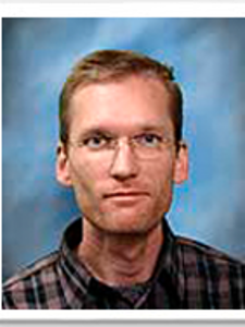
OSE Seminar by Dr. Thomas Rotter on Photonic crystal surface emitting lasers (PCSELs) based on epitaxial quantum nanostructures
Departmental News

Posted: February 18, 2025
Date: Thursday, February 20, 2025
Time: 12:45 PM to 1:45 PM
Location:CHTM Room 103 and Zoom
Speaker: Dr. Thomas Rotter, Research Professor
Center for High Technology and Materials, (CHTM)
Abstract:
Since the invention of semiconductor lasers in 1962, these devices have revolutionized a wide range of industries, from telecommunications and information technology to medical applications, by providing compact, efficient, and tunable light sources. This talk will provide an overview of recent research conducted at the Center for High Technology Materials (CHTM) related to semiconductor lasers grown via molecular beam epitaxy (MBE). I will focus on our investigations into various laser active regions designed for different wavelengths, including arsenide and antimonide quantum wells, as well as InAs quantum dots and dashes, exploring both their epitaxial growth techniques and their application in laser devices. Additionally, I will discuss our work on the design and fabrication of various laser architectures, particularly surface emitting lasers such as vertical-external-cavity surface-emitting lasers (VECSELs) and photonic crystal surface-emitting lasers (PCSELs). Each of these architectures in combination with specific active regions presents unique challenges and opportunities in terms of performance, efficiency, and integration with other technologies.
Biography:
Thomas J Rotter is a Research Associate Professor at the Center for High Technology Materials at the University of New Mexico. He currently works on projects involving the epitaxial growth of optical and electronic devices, including lasers, VECSELs, PCSELs, photodetectors, solar cells, SESAMs, and high mobility transistors. The devices are based on III-V arsenides, antimonides and phosphides and include highly mismatched materials, self-assembled nanostructures as well as low dimensional materials. He received his PhD degree in Optical Sciences from the University of New Mexico in 2007 and the equivalent of a Master's Degree in Physics from the Westfaelische Wilhelms Universitaet Muenster, Germany. He has also been working at the California NanoSystems Institute at the University of California at Los Angeles, at the Air Force Research Laboratory at the Kirtland AFB and at Actoprobe LLC. He has authored or co-authored over 90 technical papers in peer reviewed journals.
